We often see large and small holes on circuit boards. Holes can be roughly divided into PTH (Plating Through Hole) and NPTH (Non Plating Through Hole). “It’s because this kind of hole really penetrates from one side of the circuit board to the other. In fact, in addition to the through holes in the circuit board, there are other holes that do not penetrate the circuit board.
How to distinguish between PTH and NPTH
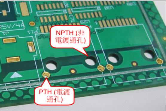
In fact, it’s very simple. Refer to the above picture, just look at the hole wall for bright plating traces to judge. The hole with plating trace is PTH, and the hole without plating trace is NPTH.
The use of NPTH (non-plated through hole):
If you save a little bit, you will find that the aperture of NPTH is usually larger than that of PTH, because NPTH is mostly used as a lock screw, and some are used to install some connectors outside the connection.
In addition, some will also design NPTH at the edge of the board (break-away) for the positioning of the test fixture. In the early days, it will also be used to fix the circuit board during SMT assembly/placement. Now most of the SMT punching machines use clamping methods instead of thimble to fix the circuit board.
Uses of PTH (Plated Through Hole):
Generally, there are two purposes for PTH holes in circuit boards. One is for welding the legs of traditional DIP parts. The diameter of these holes must be larger than the diameter of the welding legs of the parts, so that the parts can be inserted into the holes.
Via (via hole) use introduction:
Another kind of relatively small PTH, usually called via (via), is used to connect and conduct the copper foil circuit between two or more layers of the circuit board (PCB), because the PCB is made of Many copper foil layers are accumulated, and each layer of copper foil (copper) will be covered with an insulating layer, which means that the copper foil layers cannot communicate with each other, and the signal connection is via via. That’s why the Chinese call it “via”.
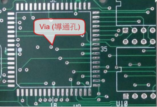
However, most of the current vias are covered with green paint (solder mask), just like the picture above, especially the mobile phone board, because the parts on the board are getting denser and denser, and some vias are even placed directly under the parts. In order to prevent the parts and vias from accidentally short-circuiting and causing quality problems, most of the vias are covered with green paint.
Because some vias have solder paste printed on them, when the board flows through the reflow oven, the solder paste is likely to flow from the via to the other side of the board and cause short circuits. Therefore, most of the current PCB processes will use the via The aperture is made small, and then covered with green paint to avoid possible quality problems in the future.
Of course, many people think that the construction method of using green paint to cover the vias is a quality risk, because there may be a risk of corrosion due to incomplete cover holes or chemical residues, but it is undeniable that the use of green paint to cover holes is still the most current. Cheap and acceptable way to fill holes.
In addition to using green paint to cover the holes, some people also use resin to fill the holes first and then cover the holes with green paint. This construction method is more in line with the quality requirements, but there is an additional process, and the cost of course has to be increased. In addition, if it is a through hole or a blind hole on the pad/pad, we generally require the use of copper plug holes, and finally the surface treatment is performed to avoid the risk of solder paste flowing into the through hole.