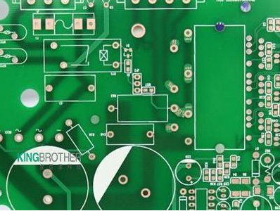
With the improvement of product performance, the PCB is also constantly updated and developed, the circuits are more and more dense, and more and more components need to be placed. At this time, if you want to drill holes in the plate, you need quite a bit of technology.
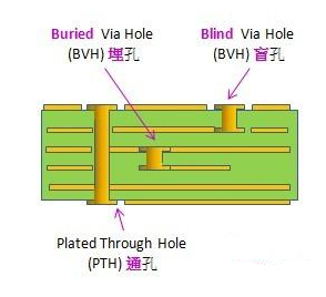
There are many kinds of PCB drilling techniques. Traditional methods are used to make blind holes in the inner layer. When successively laminating multi-layer boards, two double-sided boards with through holes are used as the outer layer and the inner layer board without holes is pressed. The blind holes filled with glue can appear, and the blind holes on the outer plate surface are formed by mechanical drilling. However, when making machine-drilled blind holes, the setting of the drill depth of the drill bit is not easy, and the bottom of the tapered hole affects the effect of copper plating. In addition, the process of making the blind hole in the inner layer is too long and wastes excessive costs. Increasingly unsuitable.
In addition to the carbon dioxide drilling and laser drilling that we have previously introduced, there are also mechanical drilling, photosensitive drilling, laser drilling, plasma etching, and chemical etching.
Mechanical drilling is made by high-speed machining. The main one is the drill bit. The drill bit generally uses tungsten-cobalt alloys. The alloy is based on tungsten carbide powder and cobalt as the binder. It is sintered at high temperature and pressure. High hardness and abrasion resistance can smoothly drill the required holes.
Laser holes are made by carbon dioxide and ultraviolet laser cutting. Gas or light forms a light beam with strong thermal energy. The copper foil can be burned through to produce the required holes. The principle is the same as cutting, mainly controlling the beam.
Plasma is also the plasma. The particles that make up the plasma are relatively large in distance and are constantly colliding randomly. Its thermal motion is similar to ordinary gas. Plasma etched holes are mainly used for the PCB of resin copper layer. Oxygen-containing gas is used as the plasma. After contact with copper, an oxidation reaction will occur, and the resin material will be removed to form holes.
As mentioned before, objects remaining on the PCB cannot be removed by ordinary methods. Chemical cleaning methods can be used to make the chemical react with the residues to remove them. The same is true for drilling. Using chemical agents, the copper foil, resin, etc. can be etched by dripping on the place where drilling is needed, and eventually a hole is formed.